The 2nm process is blocked, and the microwave oven is a key breakthrough point | TSMC & Cornell University
Author:Quantum Time:2022.09.12
Pine sent from the quantity of the Temple of Temple | Public Account QBITAI
Microwave furnaces are key technologies for making 2 nano -chip.
That's right, the microwave oven in the kitchen.

The research team of Cornell University improved the home microwave oven and used the microwave method to process the chip. It also said that it could reduce the chips of TSMC and Samsung and other leading manufacturers to only 2 nanometers.
Related research results have been published in the Applied Physical Express.

Can microwave ovens become a breakthrough point for making 2 nano -chip?
How about it, let's take a look together.
Microwave technology enhances the current conduction capacity
Prior to this, let's briefly understand what to limit the production of 2nm chips.

There will be many transistors on the chip. Inside the transistor, the current will flow from the starting end (source) to the end point (drain).
In this process, the current will pass through a gate (gate), and the width of the gate is the chip size that is usually called.
However, with the development of process technology, the width of the gate is getting smaller and smaller, and the distance between the source and the drain is getting closer and closer.
This will cause the grid to interfere with the grid of the source and leaks, which will greatly reduce the control capacity of the grille on the current, that is, the short -channel effect occurs.
The solution to the short channel effect is largely to work hard on chip materials and technology. One of the ways is to increase the device doping concentration.
Specifically, it is to activate the doped atoms by doping a lot of other atoms in chip materials and then annealing.
For example, mixing phosphorus atoms into silicon, and then heating and annealing this mixture to increase the balance concentration of phosphorus atoms, that is, activating the activity of phosphorus atoms in silicon, thereby improving its current conductivity.
But increasing the concentration of doping is not easy.
The traditional heating and annealing method of heating concentration of balanced concentration has reached the limit. If you want to improve, you may cause silicon crystal swelling.
The traditional method does not work, you can only find another way.
No, researchers of Cornell University proposed a new way to improve the balance of phosphorus: microwave technology.

△ Source: Cornell.edu
Prior to this, TSMC had already made a speculation that the microwave can activate excess doped.
But the microwave has a great weakness, that is, the existence of the waves. It does not conduct energy, which will hinder the continuous activation of doping in the material.
Then, as long as it solves the problem of "resident wave", everything will be solved.
Indeed, TSMC and Huang Zhelun, the University of Cornell University, improved the microwave oven together, so that the resident waves generated by the microwave oven during work can be effectively controlled.
In this way, the time to control the occurrence of the station can be selected, so that the atoms doped in the chip material can be appropriately activated without excessive heating and damaging crystals.
In addition, the use of microwave technology to increase doping concentration may also change the geometric shape of the transistor used in the chip.
The fins of the fins have more than 20 years, and microwave annealing has made a new transistor structure possible. In this structure, the transistor is superimposed as a horizontal nanometer, which can further increase the density and control of the transistor.
It is worth mentioning that Huang Zhelun also predicted this technology:
This technology may be used to produce semiconductor materials and electronic products that appear around 2025.
In addition, he also applied for two patents of microwave thermal artifacts with Dr. Gianluca Fabi.
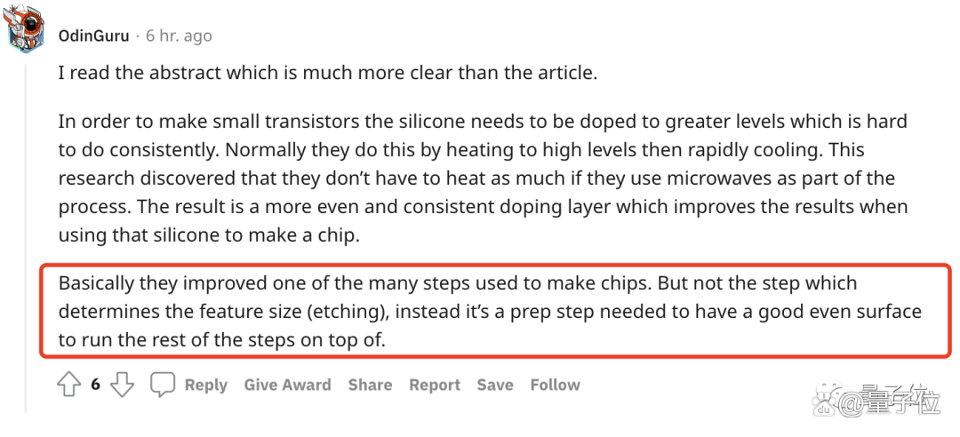
But whether the microwave technology can be regarded as the key technology to make a 2NM chip, some netizens have expressed their opinions.
Basically, they improved one of many steps for manufacturing chips. But this is not the step of chip size. On the contrary, it is just a preparation step for other steps to run better.

For microwave technology, do you think it is the key to breakthroughs in 2nm chips?
Welcome to leave a message in the comment area below ~
Thesis link: https://aip.scitation.org/doi/full/10.1063/5.0099083 Reference link: https://news.cornell.edu/stories/2022/modified-Microwave-CoOKS-NExt- -Semiconductors
- END -
E -commerce platforms can still buy women's drugs and similar products. More than one shop is a

According to the official Weibo news of the Morning News 021 Video, on June 13, se...
Astronauts have settled in the "Space Home" of China Space Station for a year!

Today, a year ago, China Space Station ushered in the first batch of Chinese astro...