Chiplet: Big and computing wings
Author:China Financial Information Ce Time:2022.08.18
Introduction to the author: Erick.x, the chief architecture expert of Fu Ruiwei.
Chiclet Overview
Over the past few decades, the semiconductor industry has been developing in accordance with the laws of Moore's law. With the iteration of the chip manufacturing process, the chip performance has doubled every 18 months. However, when the process has evolved to 5nm and 3nm nodes, the density of the transistor is becoming more and more difficult. At the same time, due to the high integration, the power consumption density is getting stronger, and the power supply and heat dissipation are also facing huge challenges. Chiclet (core grain) technology is an important way to continuously improve integration and chip computing power when Moore's law has gradually slowed down. Recently, there have been multiple products based on Chiclet in the industry. Intel has even released the Ponte Vecchio series that integrates 47 chips. Chiclet technology is already a technical means that chip manufacturers are more dependent.
Compared with the traditional Monolithic chip technology, in the context of Chiclet technology, large single -chip chips can be divided into multiple or different small chips. These small chips can be made with the same or different process nodes, and then through cross -chip interconnection and packaging technology Perform packaging level integration, reduce costs while obtaining higher integration. Generally speaking, because the size of the light carvings is limited to 33mm * 26mm, the area of a single chip generally does not exceed 800mm^2. Through the integrated between multiple chips Spend. And the Bose-Einstein model from the process manufacturing yield:
Among them, A represents the chip area, D0 represents defect density, and n represents the coefficient correlation coefficient of the mask version layer. The larger the area of the single chip, the lower the yield, and the higher the corresponding manufacturing cost. At the same time, in the current mainstream chip architecture, the signal processing part is usually digital logic. As the process evolving the same function, the area will be further reduced, but the various types of interface parts are usually analog circuits. Under the same function of process evolution, the area is area. It will hardly shrink, so it can be reasonably divided into chips that are not used to effectively divide them on different process nodes. It can more efficiently use existing manufacturing processes to effectively reduce costs.
At the same time as the above -mentioned high integration and low cost, ChiPlet technology also faces many technical challenges. Generally speaking, it can be summarized as: how to psychologically how to stitch multiple chips; how to divide large chips into multiple small chips in design ; And how to standardize the interface protocol to achieve standardized stitching of different chip products. Specifically, it can be divided into several different aspects:
Ultra -high -speed, ultra -high -density and ultra -low -latency packaging technology is used to solve the wiring density inside the single chip, high -speed reliable signal transmission bandwidth and ultra -low latency signal interaction between Chiclet. At present, mainstream packaging technologies include but are not limited to MCM, Cowos, EMIB, etc.
Based on the architectural design of Chiclet, on the one hand, consider how to divide and architectural definition between different ChiPlets, and on the other hand, consider how multiple Chiclets perform effective interconnection and expansion to achieve efficient and flexible scalability architecture, avoid signal between multiple chips and multiple chips. Functions and performance issues such as dead locks, traffic congestion.
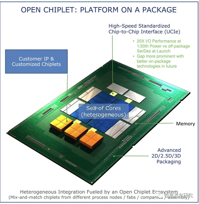
Standardized multi -Chiclets interactive communication interconnection protocols are used to guide and restrain interface design and standardized docking of different chips. Ucie (Universal Chiplet Interconnect Express), which is jointly developed and developed by Intel, AMD, ASE, Google, Meta, Microsoft, Qualcomm, Samsung, and TSMC, has released the first edition standard.
Due to space limitations, based on the above three aspects, this article briefly introduces the current mainstream implementation methods of the industry, explores the advantages and disadvantages and design considerations of different solutions, and will be attached to the detailed introduction of each part in the future.
Support the underlying packaging technology of chicklet
Packaging technology is currently dominated by companies such as TSMC, ASE, Intel, including 2D MCM to 2.5D COWOS, EMIB and 3D Hybrid Bonding. This article mainly introduces the current mainstream 2D and 2.5D packaging technology and its advantages and disadvantages of the mainstream in the industry.
1. MCM (Multi-Chip Module)
Multi-chip module
MCM generally refers to the technology that connects multiple chips through Substrate. Generally speaking, the distance and range of the wiring can be at 10mm ~ 25mm, the width is about 10mm width, and the bandwidth of a single wiring is about 10Gbit/s. Because the MCM can directly connect to each chip through the substrate, the cost of the packaging is relatively low, but because the lines of the line line are relatively wide, the packaging density is relatively low, the interface rate is relatively low, and the delay is relatively large.
2. Cowos (Chip-ON-WAFER-SUBSTATE)
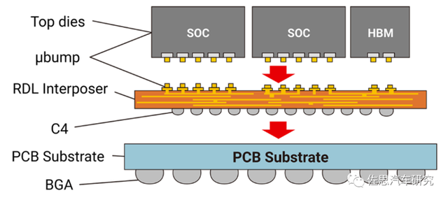
COWOS is a TSMC -led 2.5D packaging technology implemented based on Interposer (intermediate medium layer). Among them, Interposer uses a chip manufacturing process with a mature process, which can provide higher -density and higher -rate interfaces than MCM. At present, the mainstream COWOS technology of TSMC includes: COWOS-S: Basic COWOS technology, which can support ultra-high integrated density, providing the Interposer layer of not more than twice the size of the film, which is usually used to integrate high-speed high-wide memory chips such as HBM.
Cowos
COWOS-R: Based on the aforementioned Cowos-S technology, the RDL (Redistribution layer) in INFO technology is introduced. The RDL intermediary layer consists of a polymer and copper wire. It has relatively mechanical flexibility. Reliability, allows new packaging to expand its size to meet more complex functional needs, thereby effectively supporting high -speed reliability between multiple Chiplets.
Cowos-R
COWOS-L: On the basis of the above Cowos-S and INFO technology, the LSI (Local Silicon Interconnect) technology is introduced. LSI chips can have multiple connection architectures in each product (such as SOC to SOC, SOC to small chips, SOC chips, SOCs To HBM, etc.), can also be used for multiple products, providing more flexible and replicable multi -chip interconnection architecture.
Cowos-L
Compared with MCM, COWOS technology can provide higher interconnection bandwidth and lower interconnection delay to obtain higher performance. At the same time, due to the size of the interposer (usually the maximum size of the two -fold mask version), the upper limit of the packaging density that can be provided is relatively limited, and due to the introduction of Interposer, you need to pay additional manufacturing costs and higher technical complexity. And the decrease of the overall yield.
3. EMIB (EMBEDDED MULTI-DIE Interconnect Bridge)
Emib
EMIB is an Intel -led 2.5D packaging technology. It uses multiple embedded bridges that contain multiple routing layers. At the same time, it is embedded in the packaging substrate to achieve high -efficiency and high -density packaging. Since the interposer is no longer used as the intermediate medium, the TSVS that is connected to the interposer can be removed, and the restrictions of the packaging size brought by the interposer size can be obtained.
Overall, compared to the aforementioned MCM, Cowos and Info/LSI technology, EMIB technology is more elegant and economical, and obtain higher integration and manufacturing yield. However, EMIB needs to encapsulate technology with bridge connection chips, and the technical threshold and complexity are high.
Chiclet architecture challenge and insight
Based on the architectural design of Chiclet, we must first consider how to divide and architectural definition between different chips. At present, the mainstream design ideas can be roughly divided into two categories:
the first sort
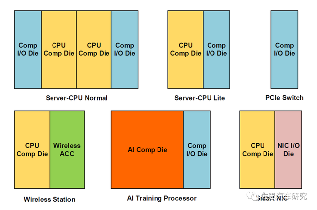
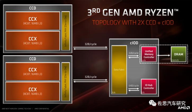
Based on the functional division to multiple Chiplets, a single Chiclet does not include a complete function set. Different types of products are encapsulated through different chps combinations. Typical representatives are the HUAWEI Lego architecture (KUNPENG & Ascend) and AMD Zen2/3 architecture.
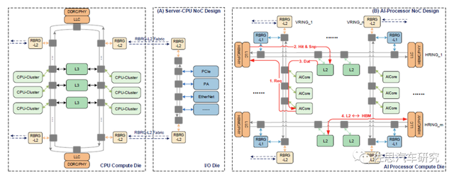
HUAWEI Lego architecture: Use Compute Die (Compute + Memory Interface) and I/O DIE combinations to disassemble different CHIPLETS functions. Adopt advanced technology during the Computer Die (CPU/AI) design, obtain top -level computing power and energy efficiency, and use mature processes when designing I/O DIE design, and obtain cost returns in the case of small area and advanced process. And the number and combination form of different chips that can be flexibly matched, thereby combining a variety of different specifications of cloud high -performance processor products.
Huawei lego
AMD Zen3 architecture: The form of CCD (Compute) and CIOD (Memory Interface + I/O) is used for different Chiclets function disassembly. In CCD design, the most advanced process is used to obtain top -level computing power and energy efficiency. In the CIOD design, a mature process is used, and cost returns are obtained in the absence of the area where the area is not much different from the advanced process. And CCD itself is designed in the form of two 4C8T CLUSTER combinations, which can meet the requirements of AMD from Desktop to Server. According to the scene of the number of CCDs and the corresponding CIOD, the flexibility is very high.
AMD Zen3
Second category
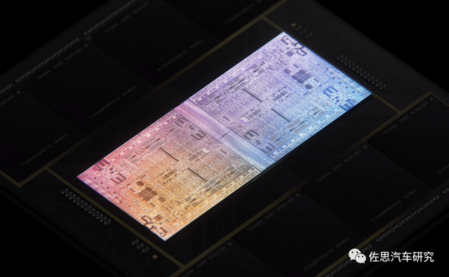
A single Chiclet contains more independent and complete functional sets, which obtains linear growth through multiple Chiplets -level couplets. Typical representatives are Apple M1 Ultra and Intel Sapphire Rapids series. Apple M1 Ultra: The packaging technology Ultrafusion, which is self -developed by Apple, stacks two M1 Max chips, so that the two chips have more than 2.5TB/s bandwidth and extremely low delay. Based on this interconnected delay bandwidth ability, M1 Ultra can directly obtain the computing power of M1 MAX directly, and at the same time, the M1 Ultra can still be treated as a complete chip without increasing the burden of adding software modification and debugging Essence
Apple M1 Ultra
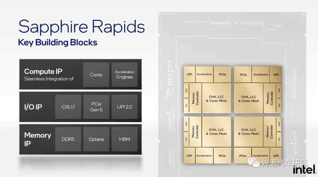
Intel Sapphire Rapids: Through the BUILDING BLOCKS of the same architecture of the two sets of mirrors, combine 4 Chiplets to obtain 4 times the performance and interconnection bandwidth. Each basic module contains calculation (CHA & LLC & Cores Mesh, Accelerateors), Memory Interface (Controller, CH0/1), and I/O (UPI, PCIe). By composing the above high -performance components to form a basic Building Block, and then use EMIB technology to interconnect, you can obtain linear performance improvement and cost returns.
Intel Sapphire Rapids
Based on the architectural design of Chiclet, it is necessary to consider how multiple CHIPLETS performs effective interconnection and expansion to achieve efficient and flexible scalability architecture, and avoid functional and performance problems such as signal deadlock and traffic congestion between multiple chips. Because the interconnection inside the chip is usually a parallel data transmission under the assumptions of reliable connection, and the interconnection between chips is usually transmitted by the serial data under unreliable assumptions. The mainstream design ideas and application scenarios are roughly divided into two categories:
the first sort
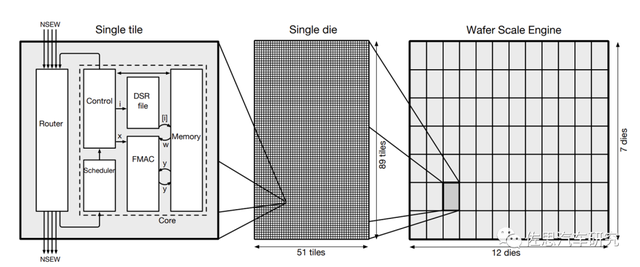
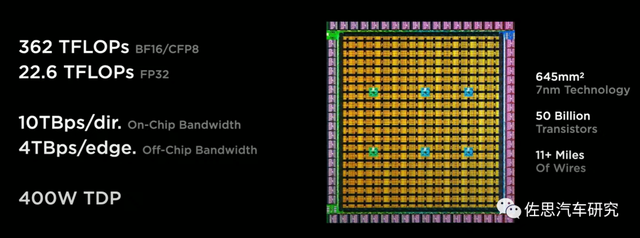
The same architecture between the film, the traffic is flat or basically flattened. Typical representatives such as CEREBRAS, using Tile to Die Die to WAFER Scale Engine. Another typical representative is Tesla Dojo. It uses Info-SOW's packaging and chip four sides to place the I/O interface to achieve 10Tbps bandwidth in each direction in the chip, 4Tbps per side, and the unilateral bandwidth 9Tbps after SOW integrated.
CS-1 WAFER SCALE Engine
Dojo d1 chip
Second category
The structure of the film is similar, and the traffic between the film converges in a certain percentage. Typical representatives are the aforementioned Huawei Bufferless Multi-Ring architecture. The traffic on the film will converge to various cross-span interfaces; another typical representative is the aforementioned Apple M1 Ultra, and the traffic on the film converges to the UltraFusion concentration exchange part.
Bufferless Multi-Ring
From the perspective of calculating the load, when a single computing task has a high density and exceeds the scope of the single -chip computing power range, multiple chips are needed to complete. In order to use computing power more effectively and improve computing efficiency. The typical task type is the training task of AI. The interconnection architecture of the aforementioned Cerebras and Dojo has a strong advantage in such scenarios. When the number of computing tasks is huge, the single task load is small, and the traffic flow is usually far less than the on -chip traffic. At this time, the traffic convergence strategy is more suitable.
From the perspective of the implementation of the interconnection architecture and the implementation strategy, it can usually be further subdivided according to the network's topology, routing strategy, and anti -death lock mechanism. This article is no longer introduced in detail due to space limitations.
Introduction
The industry has been gradually trying to gradually attempts to design Chiclet -based chip design since 2016. After a long period of exploration, it has made deep accumulation and great progress in the packaging process and architecture. UCIE 1.0, which was jointly launched by Intel, AMD, ARM, ASE, Google, Meta, Microsoft, Qualcomm, Samsung, and TSMC in March 2022.
The original intention and goal of the UCIE standard is to establish a set of reference standards such as the design and manufacturing related design and manufacturing related to the Chiclet technology, so that the chips of different design and manufacturing manufacturers can be seamlessly integrated, thereby creating a complete and flexible chip development ecosystem of the packaging level. system. Based on the Chiclet technology and UCIE standards, the chip area of the size of the single mask version can be achieved, and a higher -performance chip with a larger size and higher integration can be obtained. At the same time, the standard UCIE can enable various types of different processes and chips and IPs of different sizes to integrate at the packaging level, effectively reduce development costs, and reduce the development cycle. Figure. Initial motivation of ucie
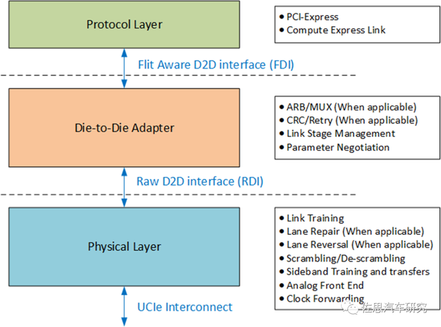
The specifications and standards specified in UCIE include the following levels (specific content is not repeated in this article):
Agreement layer: defines high -level communication protocol standards, and the initial version adopts mature PCIE plus CXL protocol.
Intermediate layer: Define the adaptation criteria between Chiplets, including LINK status management, parameter alignment, signal selection verification, and possible re -transmission mechanisms.
Physical layer: Define the standards and physical link design standards for electrical signal connections, including electrical signal definition, clock definition, LINK and SIDEBAND training.
Figure. Layering with ucie
Summarize
In summary, after several years of development, Chiclet technology has gradually moved towards maturity and commercial use, becoming a technical means that chip manufacturers are more dependent on, and it is also considered an important direction for the development of the chip industry in the future. At the current encapsulation level, there are already manufacturers such as TSMC, Intel, and other manufacturers provided COWOS, EMIB and other advanced packaging, which can provide Chiclet interconnection with ultra -high -speed, ultra -high density and ultra -low lattice; at the standard protocol level, many large manufacturers have led the release of release. Ucie 1.0 version provides guidance and constraints of cross -chip interface design. At the level of architecture design, how to design high -performance, high efficiency, flexible and scalable interconnection architecture based on Chiclet, and how to divide the functions between chips based on the realization and business perspective is still the biggest challenge in Chiclet technology.
Reference:
https://3dfabric.tsmc.com/english/dedicatedFoundry/technology/3dfabric.htmmm
https://ase.aseglobal.com/public/en/technology/focos.html
https://www.intel.com/content/www/us/en/silicon-novations/6-pillars/emib.html
S. Naffziger, K. Lepak, M. Paraschou, and M. Subramony, “2.2 amd chiplet architecture for high-performance server and desktop products,” in 2020 IEEE International Solid-State Circuits Conference-(ISSCC). IEEE, 2020, pp. 44–45
A. BISWAS, "Sapphire Rapids," in 2021 IEEE HOT Chips 33 Symposium (HCS). IEEE Computer Society, 2021, PP. 1–22.
T. Wang, F. Feng, S. Xiang, Q. Li and J. Xia, "Application Defined On-chip Networks for Heterogeneous Chiplets: An Implementation Perspective," 2022 IEEE International Symposium on High-Performance Computer Architecture (HPCA), 2022, PP. 1198-1210, Doi: 10.1109/HPCA53966.2022.00091.
https://www.apple.com/tn/newsroom/2022/03/Apple- Unveils-m1-Ultra-worlds-most-powerful-chip-A-Personal- Computer/
watch? v = j0z4fwecy4m
Yin, jieming, et al. "Modular Routing Design for Chiplet-Based Systems." 2018 ACM/IEEE 45th Annual International Symposium on Computer Architecture (ISCA). IEEEE, 2018.
https://www.uciexpress.org/specification
Xia, jing, et al. "Kunpeng 920: The First 7-NM Chiplet-Based 64-Core ARM SoC for Cloud Services." IEEE Micro 41.5 (2021): 67-75.
https://www.anadtech.com/gallery/album/8123 #3
- END -
The world's first one!This Hubei Medical Remote Sensing Satellite is scheduled to launch next year

In the vast spaceA new satellite will be added next yearThis satellite is also the...
Douyin, station B stealing each other?
As the traffic growth of the domestic mobile Internet grows saturated, the income ...


