The stuck neck is added, the United States breaks EDA
Author:Arai Telescope Time:2022.08.14

▍ Salt Finance
Author | Xiangyi
Edit | Fry
Following the signing of the "Chip Act", in the past two days, the United States has sacrificed a major killing trick to "absolutely control" the chip industry.
On Friday, the US Department of Commerce announced that the exports of 4 technologies were restricted, of which 3 were related to semiconductor.
These four technologies are: pressure gain technology that can be used for rockets and hypersonic systems; the fourth -generation semiconductor materials that can withstand high temperature and high voltage are oxidized and diamonds; ECAD software designed for 3nm and below chips.
After being included in the list, the exports of these four technologies need to apply to the US Department of Commerce for export permits. In this regard, the reason given by the US Department of Commerce is "for national security considerations."

The U.S. Department of Commerce announced that the export of 4 technologies has limited, and 3 of them are related to semiconductor
This time the export control ban did not clearly mention China, but it is obvious that this is a supporting measure for the American "chip bill" and strategy. The purpose is to curb the progress of American competitors in the chip field, especially advanced cutting -edge chip technology.
The main competitor of the American sword finger is of course China.
The upstream of the industry is "blocked"
Among the four technologies listed in the list, the most concerned is "the EDA software for the development of the GAaFet structure".
This also means that the United States' technical blockade of mainland China extends from "chip manufacturing" to "chip design".
The production process of a chip has four main links: design, manufacturing, packaging and testing.
Obviously, this time the US technology blockade has been "more upper level", which approached the upstream of the chip industry chain.
The chip design is inseparable from the EDA software. In a metaphor, just like the field of architecture and electrical design, the drawing software CAD is inseparable.
"If the EDA tool is completely lost, the integrated circuit chip will not be able to continue to mass production on a large scale."

Chip design is inseparable from EDA software
Similar to the ground building, the design of the chip circuit diagram is like designing a high -rise building on the silicon wafer, which eventually develops into a city group that can operate.
However, its scale is much smaller and more precise.
In the 1970s and 1980s, engineers used hand -drawn drawings when designing chips.
As the chip complexity increases, manpower can no longer meet the chip tens of billions of transistor design and manufacturing projects, and the assistance of EDA software must be used.
EDA's full name is translated as "Electronic Design Automation", but the conspiracy research and analyst Junman told Salt Finance that the role of EDA auxiliary is not just the design of the design, "it runs through the entire integrated circuit design, production, manufacturing process" Essence
"(For circuit diagrams) analysis, optimization and verification are accompanied by design. The chip design process itself is design, analysis, optimization, and verification repeated iteration." Shang Junman said that in the chip design industry, there is "one step and one verification" in the chip design industry. The statement, that is, the advancement of each step of design steps If there is a violation or dissatisfaction with the design needs, it must return to iteration and repeat the previous step until it meets the needs.
At the same time, in addition to the most mainstream design for EDA tools, there are also EDA tools used in wafer manufacturing, seal testing and other links. The wafer manufacturing EDA tool is used to support process development, device model, mask design, and yield analysis.
Therefore, EDA does not refer to a certain software, which is a collective name of a type of software.
In the chip production link, different chips and processes need to use different EDAs.
According to Shang Junman, from the perspective of process coverage, EDA can be divided into single -point EDA tools and process EDA tools (can be broadcasted to the full process EDA tool).
As the origin of semiconductor technology, the United States has an absolute advantage in the EDA field.
In the global EDA market, SynopSys, Cadence and Siemens EDA account for 70%; in the Chinese market, the market share of these three EDA companies is about 78%.
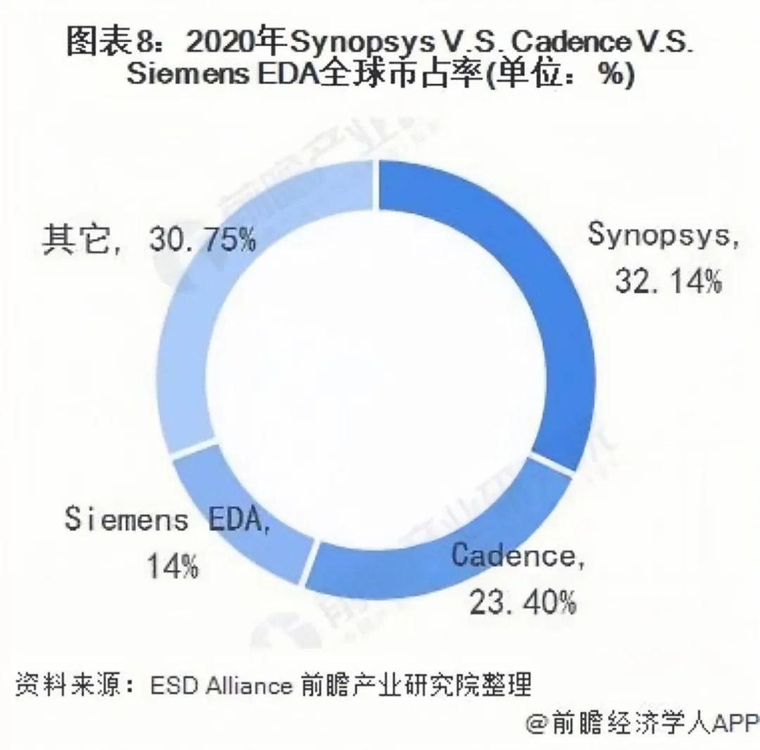
In the Global EDA market, SynopSys, Cadence, Siemens EDA, three companies account for 70%
Therefore, the US government's dyeing of EDA technology is undoubtedly a "throat" behavior.
In conjunction with the recent actions such as the "Chip Act", Shang Junman believes that this shows that the United States has played a card in the field of iconic types of Chinese chip wars.
Once the siege of publicity in advance
The United States attempts to become a "chip manufacturing" place again, which is obvious. Therefore, it can be said that the emergence of EDA cards did not surprise the industry.
The question is, when does it appear and how much does it have?
At present, the goal of the US government is obvious: on the one hand, maintaining its own technical advantages; on the other hand, the exploration of advanced technology that competitors may initiate for advanced technology will be "closed" in advance.
As mentioned earlier, EDA is a collective name for different software, and the list of the US Department of Commerce is only "EDA software used to develop GAAFET structures."
What is "GAAFET structure"?
To understand simply, the "GAAFET structure" is a foundation for advanced processes to 3nm and below.
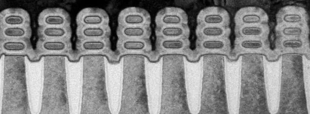
GaaFet cross section
We know that the normal operation of logical circuits mainly relies on the precise control of electrons in semiconductor units. Before the 20nm process, the plane structure Planar Fet was the mainstream technology. However, after moving towards the advanced process, the transistor is getting smaller and smaller, which means that the channel contact area is also becoming smaller, and the control of the current becomes unstable.
Therefore, at that time, the alternative technology was the FinFET structure transistor. Among them, FIN (fin) extended, increasing the channel contact area, and increased the effective width of the control current.
But the process continued to improve, and the FinFET structure also appeared in shortcomings. Therefore, in the 3nm and below process, the GaaFet structure is regarded as a solution.
It is currently known that Samsung Propaganda will use GaaFet in the 3nm process, while TSMC announced that it will be exchanged for 2nm processes before using GaaFet.
Samsung Propaganda will use GaaFet in 3nm process
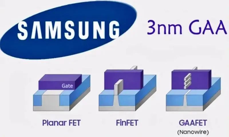
Therefore, the GAAFET structure is the "pass" of the advanced process.
Therefore, this time the US Department of Commerce has only 3nm and below advanced processes, which has a relatively limited impact.
"The existing common chip design process in China has not yet reached 3mm and below." Shang Junman said to Salt Finance that the policy focused on "the future", not "the present".
At present, only 3nm and below players are only Samsung in South Korea, TSMC in Taiwan, and Intel in the United States.
However, Shang Junman said that in the long run, if the United States continues to make an analing Activity EDA tool, Chinese chip design companies will be blocked to higher added value and stronger technical capabilities, and the difficulty of breakthroughs in advanced processes will plus the difficulty of plus the difficulty of the breakthrough of advanced processes. big.
The organs are exhausted, the anti -injury itself
At this point, the scope of the impact of new technical controls has clearly clearly influenced in mainland China. "Although there is no close worry, there is far -sightedness."
However, the perspective of the horizon, especially from the perspective of the United States, is not only the power of the above technical control.
On August 9, US President Biden signed the "Chip Act". The bill stipulates that the U.S. government will provide more than $ 50 billion to expand the share of chip manufacturing in the United States.
On August 9, 2022, local time, the U.S. capital Washington, DC, US President Biden signed the "Chip and Science Act" in the White House

Although semiconductor technology started in the United States, in the 1970s and 1980s, chip manufacturing was gradually shifted. First, Japan, then South Korea and Taiwan.
To this day, the strategic significance of the semiconductor industry is particularly prominent, and a "arms race" has already begun.
The United States urgently needs chip manufacturing "backflow", which is known to all passers -by.
Not long ago, Pelosi, the "third figure" of the US government, visited Asia. Whether in Singapore, South Korea, or visiting Taiwan, they did not let go of the opportunity to meet the local semiconductor leaders.
However, in fact, under the coercion of the U.S. government's request for the "selection station", semiconductor heads in various regions were placed in embarrassment.
Taking South Korean semiconductor giants Samsung and Hynix semiconductor as an example, on the one hand, they have been lobbying to the United States to build factories at a high cost; on the other hand, the premise of obtaining US subsidies is to accept "exclusive clauses" against China.
The United States has industry leadership, so that the giants have to follow, but on the other end, the giants cannot give up the market in mainland China. Samsung and Hynix Semiconductor also have nearly half of the production capacity in China, which has even increased the risk of "selection stations", causing difficulties.
Compared with the "high investment and low yields" in the United States, the subsidy of the US government is actually "a business -saving".
On the surface, the size of more than $ 50 billion given by the US chip bill is not large, but in the semiconductor field, TSMC is used as an example, and the annual investment will exceed 40 billion US dollars. So how much can the US subsidy be divided by each family?
TSMC's annual capital investment exceeds more than 40 billion US dollars
As the giants were embarrassed, the United States continued to increase "technical control", showing its teeth. Maybe we can understand that these cards are not just for "competitors" to see, it is also a bargaining chip spread to "friends".
Back to the sense of technical restrictions on our country, although it has a small impact at present, "EDA’ s localization "should undoubtedly be quickly whipped.
Shang Junman told Salt Finance that he was optimistic about the localization of EDA tools. "One of the reasons is that one of the key difficulties in the previous development of EDA companies in China is that customers are unwilling to use, resulting in product iteration and collaborative upgrades. Driven by demand, the willingness to use domestic EDA tools to use domestic EDA tools is relatively enhanced, and applications will in turn drive the development of domestic EDA enterprises. "
However, due to high technical thresholds, many categories, scarcity of professional talents, Shang Junman also said that domestic EDA is still at a level with a low market penetration rate, and its localization will be a relatively long process.
Earlier report: Just now, the United States passed a black mind bill
Capture | Yang Jun
Welcome to the circle of friends without reprinting without authorization
wx_fmt = png "data-nickName =" Salt Finance "data-alias =" nfc-yancaiJing "data-signature =" only write financial text with conscience and curiosity. "Data-from =" 0 " /> points

- END -
I found new bacteria, can I name Wang Xinling bacteria?

If you don't know the friend below, it can be called Long Mao Black Pig.In fact, i...
Human intelligence is not equal?Brain scientists say that

AI, deep learning, autonomous driving, brain interface ... we are entering a futur...